CS/EE 3710 - Computer Design Lab
Fall 2010
General Information
- Instructor: Erik Brunvand, MEB 3142, 581-4345
- Classes: T,Th 3:40pm - 5:00pm, Lectures in WEB 110,
Labs in School of Computing DSL (MEB 3133)
- Erik's Office Hours: After class, when my door is open, or by appointment
- TA: Michael Kingston
- TA Office/Lab
Hours: Monday and Wednesday 3:00-5:00 in the DSL (MEB 3133)
- Textbook: None. I'll hand out notes about the project.
- Class Mailing List: 3710@list.eng.utah.edu goes to the entire
class.
- Prof. and TA Mailing List: teach-3710@list.eng.utah.edu will send
email to both the instructor and TA. Please use this list rather than sending email
directly to Prof. Brunvand or the TA unless you have a specific reason to
send the email to only one person.
- Prerequisites: CS3700 (digital design) and CS3810 (computer architecture) or
equivalant
College Guidelines
College guidelines for adding, dropping, and other administrative
issues can be found
here.
Course Objectives
This is a laboratory class in which groups of students (groups can be
of size 3 or 4) design, build, and test a simple computer. The idea
is to use your digital design skills from 3700, and your computer
architecture knowledge from 3810, and put it all together into an interesting
semester-long project. You will receive the design specifications in lectures. You will then interpret the specifications and develop a model of the design using a combination of Verilog and schematics. The model should be simulated. Once validated you will synthesize the design onto the FPGA boards. The design will contain the instruction set design, memory organization, ALU design, control, and input-output design.
We are going to implement a 16-bit microprocessor based loosly on the CR16A Microprocessor (more details below). I'll hand out a baseline instruction-set that every team will have to implement. Subsequently, each team will augment their instruction set depending upon the type of applications they have in mind.
In addition to the basic processor design, each student team will develop IO + memory interfaces, along with necessary drivers that will control the interfaces. Moreover, each team will propose further extensions to their designs for particular targeted applications. You will have enough leverage to come up with your own applications and extensions. For example, you can develop games, do some graphics/visualization (VGA interfaces), audio signal processing (interfacing audio CODECs), study and implement basic pipelining, or design fast/efficient arithmetic components. The choice is yours. Make sure that your extensions somehow relate to your applications, and make sure you're having fun!
One of the main deliverable of this class is to design an application to run on your processor. Many students have designed games as the software that runs on the CPU: these have included a game of skiers trying to ski down a slope while avoiding abstacles, rock-paper-scissors, ping-pong, tank battlefield, among many other configurable and modular games. Students have also designed music synthesizers, applications to control stepper motors and such. Sometime around the first/second week of October, each group of students will decide on an application.
We will have a mid-semester presentation on what you have done so far (what, how, why, problems faced, workarounds, etc.) and what application you intend to design on your CPU. Once decided, then you will proceed towards writing assemblers + software for your code. Each group, and every member of the group will have to make a presentation to the class.
Course Deliverables
You will submit a final report at the end of the semester, make a presentation to the whole class, and demonstrate a functioning design. There will be one exam, probably some time towards the end of the semester, to make sure that every team member has a good understanding of what's going on in the class.
Grading
- Grading breakdown:
- Labs and checkpoints: 35%
- Mid-semester presenation: 10%
- Final Project: 50%
- Written Documentation: 20%
- Project details: 30% (project meetings, project functionality, implementation, team member evaluation)
- Group Evals: 5%
- Incompletes: Incomplete grades are only possible if you have a documented medical or legal emergency
Assignments / Labs
- Review Assignment: This assignment will cover material that I think you should have learned in CS/EE 3700 and CS/EE 3810. If you can't remember this stuff, these are the areas where you need to refresh your memory. If you have no idea about this stuff, you'll struggle in the class! Due Thursday, September 2nd at 3:40 (hand in during class).
- Finite
State Machine Lab: Tbird Turn Signals
mapped to the Spartan-3E board. This is the same Tbird
assignment as last semester in 3700, but mapped to the Spartan-3E
board. Check out the tutorial on using ISE 12.2 with the Spartan-3E
board. There are other tutorials on the CS/EE 3700 web site too. Due Thursday, September 9th,
5:00pm.
-
Tiny
MIPS processor: In this lab you'll
use the mips.v code from CMOS
VLSI Design by Weste and Harris. I'll also give you exmem.v which is Verilog code that
describes memory that can be implemented as block RAM on the
Spartan-3E part. Finally, I'll give you fibn.asm, an assembly program that
computes the n-th Fibonacci number, and the corresponding fib.dat file with the machine encoded
version that you can use to load the Block RAM. The details of this MIPS process
are found in Section 1.7 of CMOS VLSI Design. I've handed
out hard copies of that section in class. Due Thursday, September 23rd,
5:00pm.
You'll have to modify things in three ways (as described in the upcoming lab handout)
- Add an add-immediate (ADDI) instruction to the processor
- Add simple memory-mapped I/O to the switches and LEDs of the Spartan-3E board
- Write a new Fibonacci program that computes the
first 14 numbers (starting at 0), stores them in memory, and then retrieves those numbers using the switches and LEDs
- Demonstrate the new Fibonacci code running on the Spartan-3E board
-
Forming Groups: Here is a form you can use to tell us who is in your group.
Due Thursday, September 23rd, 5:00pm.
You can send this in by email also to teach-3710@list.eng.utah.edu
- VGA Controller: In this lab you'll generate a simple VGA controller to display information on a standard VGA display. You'll demonstrate a simple interface that paints the entire screen in a color that is controlled by switches on the Spartan3e board, and also a version of your Tbird state machine that displays its output on the VGA screen. Due Thursday October 7th, 5:00pm. Note that the handout says Sept 30, but I changed that based on class discussions...
- Checkpoints: From here on out you'll be working in groups on your
processor projects. We'll schedule group meetings with each group to
monitor your progress. You'll need to check off a series of
checkpoints to demonstrate that progress. I haven't put a specific
schedule on these checkpoint so that your group can set your own
timetable, but if you start falling behind I may put specific time
tables in place on a per-group basis.
At a couple places in the semester we'll also schedule in-class
presentations by each group about their project. There will be one
such presentation in mid October, and another late November.
-
Checkpoint #1: In this checkpoint you'll document your register file
and ALU. Details can be found here.
-
Checkpoint #2: In this checkpoint you'll document your complete
datapath including a connection to Block RAM, some very basic memory
mapped I/O, and a plan for your final memory solution. Details can be found here.
-
Checkpoint #3: In this checkpoint you'll demonstrate your
instruction decoding and how it interacts with your
datapath. Details TBA.
-
Checkpoint #4: In this checkpoint you'll document your control
finite state machine that is controlling everything. At this point
you should be able to demonstrate code running on your
processor. Details TBA.
-
Checkpoint #5: In this checkpoint you'll document your I/O system
and how it works with your processor. VGA, UART, PS/2 keyboard,
mouse, audio, analog/digital, etc. are all possibilities. Details
TBA.
-
Final Report and Demo: Here is a
description of the final report and documentation There are
three parts to the final report:
- Demo Day! I'd like each team to set up their project in the
DSL on Thursday December 9 from 3:40-5:00 (i.e. class time on the last day of class)
so that we can invite people in to see what you've been up to. As
part of the demo your team should prepare a poster that
describes the interesting parts of your project.
- Final Project Paper: This is a conference-style paper,
two-column, in ACM Proceedings format, no more than 8 pages, that
describes your project and your demo. See the handout for more details. The
paper format
can be found here in both Word and LaTeX templates. Due Wednesday, December 15, 5:00pm This
should be handed in as hard copy.
- Final Project Data: This is a collection of Verilog,
schematics, code listings, user guides to your application, user
guides for your assembler, and other documentataion about your
project. See
the handout for more details. Due Wednesday, December 15, 5:00pm This
can be handed in as hard copy or on-line. Please include a README
file that says what everything is.
- Group Evlaution Form This is a form you
should use to evaluate you and your group in terms of what everyone did. Every
group member should fill out their own copy of the form and turn it in
separately. This is a confidential evaluation where you can tell me how well
you think the rest of your group did. You can turn it in via email or
by hardcopy. Due on Wednesday Dec 15th.
- Class evalution form This is a form you can
use to give me confidential feedback on how you think the class went this
semester. Let me know what you liked and didn't like, what worked, and what
could have worked better. You don't need to sign this form! You can
turn it in to the SoC office, or slip it under my door when I'm not
here.
Lecture Schedule (for the last part of the semester...)
- Week of October 25th: Lectures in class.
- Tuesday - Dan Parker on Verilog Programming in Industry - Here are Dan's slides - two to a page in PDF
- Thursday - Quinton Williams and Ian Jenson on an LCC-based C compiler for the 3710 architecture
- Week of November 1st: Meetings with each group
- Tuesday, Nov 2
3:40-4:00 - Group1 (Team America) - Andrej, Marty, Paymon, Sean W.
4:05-4:25 - Group2 (Coolbeans) - Greg, Simon, Philip, Bryon
4:30-4:50 - Group3 (Teal) - Anh, Jared, Tong, Paul
- Thursday, October 21
3:40-4:00 - Group4 (Blue) - William, Jacob, Ashton, Matthew
4:05-4:25 - Group2 (Incognito) - Eyad, Sean J., Willis, Erik
- Week of November 8th: In-class presentations by each group.
- Tuesday, Nov 9
3:40-4:00 - Group1 (Team America) - Andrej, Marty, Paymon, Sean W.
4:05-4:25 - Group2 (Coolbeans) - Greg, Simon, Philip, Bryon
4:30-4:50 - Group3 (Teal) - Anh, Jared, Tong, Paul
- Thursday, Nov 11
3:40-4:00 - Group4 (Blue) - William, Jacob, Ashton, Matthew
4:05-4:25 - Group2 (Incognito) - Eyad, Sean J., Willis, Erik
- Week of November 15: Meetings with each group - Slightly Modified Schedule!
- Tuesday, Nov 16
3:40-4:00 - Group3 (Teal) - Anh, Jared, Tong, Paul
4:05-4:25 - Group1 (Team America) - Andrej, Marty, Paymon, Sean W.
4:30-4:50 - Group2 (Coolbeans) - Greg, Simon, Philip, Bryon
- Thursday, Nov 18
3:40-4:00 - Group2 (Incognito) - Eyad, Sean J., Willis, Erik
4:05-4:25 - Group4 (Blue) - William, Jacob, Ashton, Matthew
- Week of November 22: Lecture
- Tuesday November 23: Exploring the Other Devices on the Spartan3e Board
- Thursday November 24: No Class - Thanksgiving
- Week of November 29: Meetings with each group - Slightly Modified Schedule!
- Tuesday, Nov 30
3:40-4:00 - Group2 (Coolbeans) - Greg, Simon, Philip, Bryon
4:05-4:25 - Group3 (Teal) - Anh, Jared, Tong, Paul
4:30-4:50 - Group1 (Team America) - Andrej, Marty, Paymon, Sean W.
- Thursday, Dec 2
3:40-4:00 - Group2 (Incognito) - Eyad, Sean J., Willis, Erik
4:05-4:25 - Group4 (Blue) - William, Jacob, Ashton, Matthew
- Week of December 6th: Open lab day and DEMO DAY!
- Tuesday December 7th: Demo planning and last minute demo prep in the DSL
- Thursday, December 9th: DEMO DAY from 3:40-5:00pm in the DSL!!!
- Tuesday December 14th: Final documentation due...
Slides
- Introduction to CS/EE 3710: as PDF, six slides to a page, and two slides to a page
- Introduction to the CR-16: as PDF, six slides to a page, and two slides to a page
- Verilog Review: as PDF, six slides to a page, and two slides to a page
- Verilog Examples: as PDF, six slides to a page, and two slides to a page
- Mini-MIPS description (see Lab 2): as PDF, six slides to a page, and two slides to a page
- Info about the innards of the Xilinx Spartan3E FPGA chip, six slides to a page, and two slides to a page
- Slides about displays and VGA: as PDF, six slides to a page, and two slides to a page
- Slides about other I/O on the Spartan 3e board: as PDF, six slides to a page, and two slides to a page (updated 11/21/10)
Information
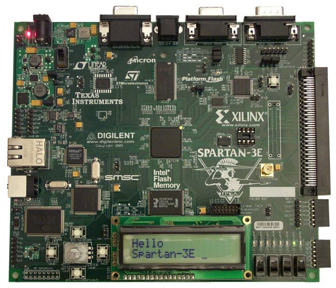
- Xilinx Boards: We'll be using the Spartan3-E "starter" board from Xilinx this semester. This is a very powerful board that includes the following:
- FPGA: Spartan-3E FPGA (XC3S500E-4FG320C)
- 500,000 gate equivalents, plus 40Kbytes of onboard RAM
- Clock: 50 MHz crystal clock oscillator
- Memory:
- 128 Mbit Parallel Flash
- 16 Mbit SPI Flash
- 64 MByte DDR SDRAM
- Connectors and Interfaces:
- Ethernet 10/100 Phy
- JTAG USB download
- Two 9-pin RS-232 serial port
- VGA output connector
- PS/2- style mouse/keyboard port, rotary encoder with push button
- Four slide switches
- Eight individual LED outputs
- Four momentary-contact push buttons
- 100-Pin expansion connection ports
- Three 6-pin expansion connectors
- Display: 16 character - 2 Line LCD
- Details of the board can be found here in the Spartan-3E Starter Kit User Guide
- Here is the Spartan-3E Family Data Sheet for the FPGAs
- Here is the Spartan-3E Family User Guide for the FPGAs
- In this directory you can find all sorts of documentation from Xilinx about various aspects of the Spartan-3E
- There are LOTS of interesting documents in that directory. A few examples are:
- In this directory you can find a number of reference designs (examples) from Xilinx using our board
- Of particular interest is the NOR-Flash Programmer project that you can use to upload data to the 16MByte parallel NOR Flash on the Spartan 3e board.
- There's also a project that demonstrates how to use the rotary encoder knob on the board
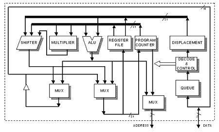
- Baseline processor architcture: Our baseline Instruction Set Architecture (ISA) is based on the National Semiconductor CR-16 microcontroller.
- Here is the CS/EE3710 ISA which is a subset of CR-16 with simplified instruction encoding
- Here is a link to the actual CR-16 definition from National (note that this is mostly for information, we will be starting from the CS/EE 3710 version above)
- Xilinx ISE WebPACK tools: We'll be using the free ISE WebPACK tool from Xlinx for design entry, synthesis, simulation, and mapping the design to the Spartan-3E board. We'll be using the latest version, v10.1.
- Verilog: We'll be using Verilog as a hardware description language this semester. I'm not requiring a Verilog text, but there are lots of good ones out there. Some books that are recommended (and are available at the Marriott Library) are:
- Verilog Digital System Design - by Zainalabedin Navabi. (Good description of event driven simulation, blocking and non-blocking assignments, and other basic concepts.
)
- Verilog HDL : A guide to digital design and synthesis - Samir Palnitkar. Priyank Kalla, who has taught 3710 a number of times, highly recommends this book
- Verilog Styles for Synthesis of Digital Systems - David R. Smith, Paul D. Franzon. These Professors have developed high-quality advanced Courses on Verilog Design, CAD & Synthesis.
- Appendix A in CMOS VLSI Design (3rd ed.) by Neil Weste and David Harris is a nice compact description of Verilog, and how various Verilog constructs map to hardware
- There are also lots of places on the web to get Verilog information
- Other
Information
- Here is a datasheet for the
32kx8 5v SRAM parts that we have. NOTE: As these are 5v parts and
you CANNOT put 5v signals back into the FPGA, you will need to use
300-400ohm series resistors on EVERY signal that will drive data
back to the FPGA if you use these chips. See the section in the
Spartan3e Starter Kit User Guide on Voltage Compatability on page 42 for an
example of interfacing to a 5v part on the Spartan3e board. To use
these chips you would wire them on a proto board or wire wrap board
that connects to the 100-pin (43 usable I/O pins) connector on the
right side of your board. Check with Travis in the DSL if you'd like
to check one of these extender boards out along with some SRAM
chips.
-
Here is a datasheet for a chip that
contains 8 separate resistors that you can use for interfacing the
SRAM data path with the Spartan FPGA.
- Here is a site with
lots of information about PS/2 keyboard and mouse
interfaces.
- Here is a site
with lots of VGA timing information.